
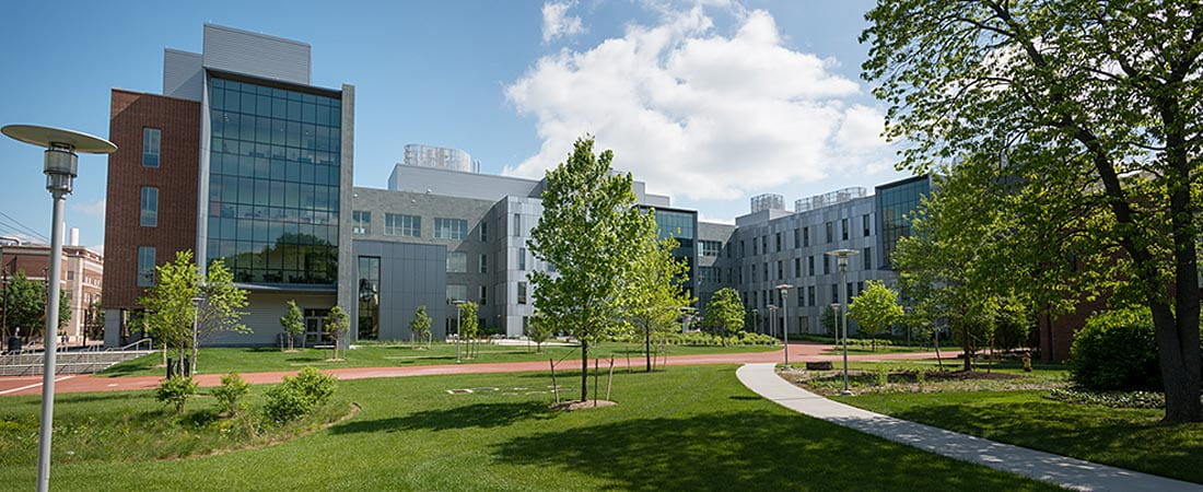
What we do
The University of Delaware Materials Growth Facility (MGF) primary objective is to provide the infrastructure, equipment, and staff support necessary to enable existing faculty, new faculty, and academic and corporate partners to undertake competitive research and development in the growing number of materials, science, and engineering fields.
Capabilities
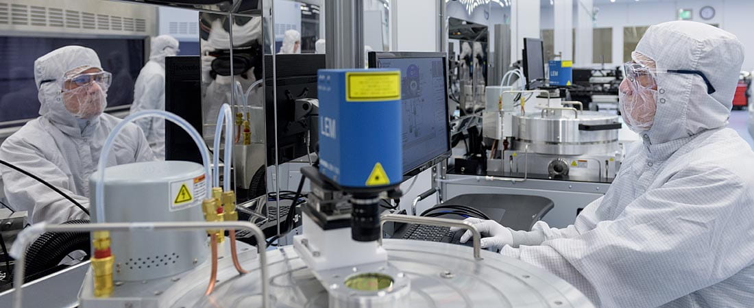
Our III-V molecular beam epitaxy (MBE), chalcogenide MBE, and magnetic sputtering system include many unique capabilities.
Services
Our staff offers full-service material calibration and growth, as well as training to perform MBE and/or sputtering deposition.
Staff
The Materials Growth Facility (MGF) is staffed by experienced professionals dedicated to serving the needs of our users. Meet our staff.
Materials Research
The Materials Growth Facility (MGF) enables cutting-edge research in fields ranging from biomedical diagnostics to quantum computing.

Core Partnerships
Collaboration across disciplines is a hallmark of research at UD and the MGF utilizes and hosts several facilities across campus. Which include:

Advanced Materials Characterization Lab
The UD Advanced Materials Characterization Lab (AMCL) provides opportunities for researchers with in the UD community as well as other Educational Institute and Industry. Equipment list includes: X-ray diffraction, thermal analysis, porosity & particle size, vibration, and mass spectrometry.
Keck Center for Advanced Microscopy & Microanalysis
The Keck Center is located in the Harker Interdisciplinary Science and Engineering (ISE) Laboratory. It houses two 200 kV field emission transmission electron microscopes JEM-2010F and Talos F200C, a LaB6 300kV TEM JEM-3011, an FEI 120kV Tecnai G2 12 Twin TEM, two scanning electron microscopes (JSM-7400F and AURIGATM 60 CrossBeamTM, with the AURIGATM 60 being a FIB-SEM dual beam instrument), and two scanning probe microscopes.
Nanofabrication Facility
The UD Nanofabrication Facility (UDNF) includes equipment and infrastructure necessary to fabricate devices at a nanometer scale. The UDNF has world-class capabilities in the areas of lithography, deposition, etch, thermal processing, characterization, and device packaging. The 8,500-square-foot clean room is divided into Class 100 and Class 1000 spaces.

Leading the Way
The Materials Growth Facility (MGF) is led by the Director Joshua Zide (left), Co-Director Stephanie Law (right) and Epitaxy Engineer Christopher Schuck (middle). The parent organization for the MGF is the Delaware Institute for Materials Research (DIMR) and is staffed by experienced professionals dedicated to serving the needs of our users.
Contact Us
If you need further assistance or are have a specific request, please fill out the form below and we will get back to you shortly.