
The MGF hosts several research groups

Doty Group
Matthew Doty, Professor
Department: Materials Science and Engineering
Dr. Doty’s research group uses nanostructure fabrication and optical spectroscopy techniques to probe and control photons, charges, and spins in nanostructured materials. Their goal is to understand how nanometer scale structure and composition can be engineered to create new materials with optimized properties. They have developed expertise in the investigation of single nanostructures. The potential for the materials they study range from next-generation computing devices to high-efficiency photovoltaics.

Jungfleisch Group
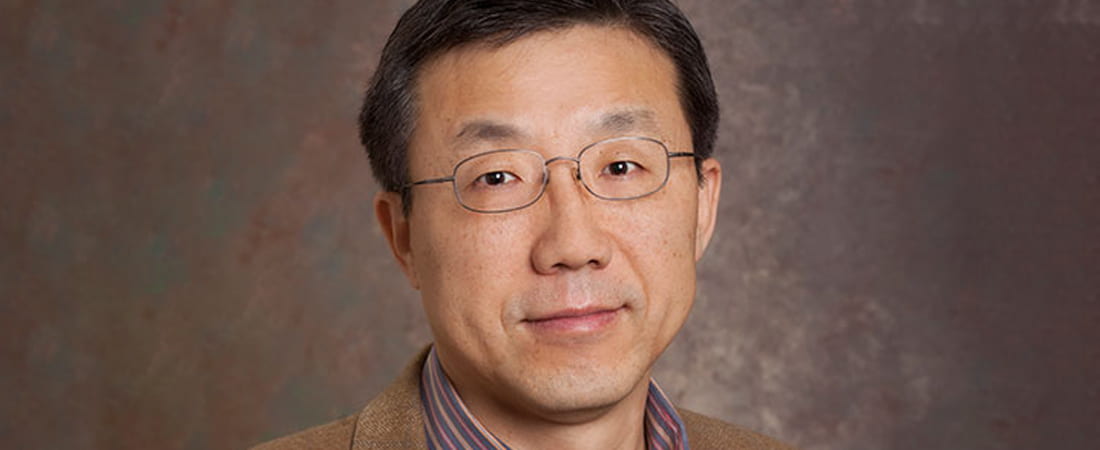
Benjamin Jungfleisch, Assistant Professor
Department: Physics and Astronomy
Dr. Jungfleisch’s group is interested in a wide range of magnetism-related topics including novel phenomena in nano-magnetism, spin-transport studies, ultrafast spintronics, and magnetization dynamics in nanoscale materials. They use advanced nanofabrication, microwave and Brillouin light scattering spectroscopy to probe magnetic interactions and excitations and understand the underlying physics in the nanostructures.

Law Group
Stephanie Law, Associate Professor
Department: Penn State University – Materials Science and Engineering EMS Energy Institute
Dr. Law’s research group focuses on understanding and synthesizing quantum materials and heterostructures to realize devices with novel, designer photonic properties. Most of their research focuses on working with long wavelength light from the mid-infrared through the terahertz. Our materials can squeeze light into tiny volumes, make light bend backward, and slow light down. These devices have applications in thermal and biological imaging, infrared and terahertz detectors, chemical sensing, environmental monitoring, security and defense, and quantum computing.

Optoelectronic Devices Group
Jamie Phillips, Professor and Department Chair
Department: Electrical and Computer Engineering
The Optoelectronic Devices Group is investigating new optoelectronic devices for the next generation of infrared systems, solar photovoltaics, and energy harvesting devices for the Internet of Things. They are exploring optoelectronics based on new semiconductor materials and innovative device architectures. Their research includes InP based infrared detectors, photovoltaic energy harvesting for mm-scale systems, and infrared spectral filters.
Electromagnetic Materials Research Laboratory
John Q. Xiao, Unidel Professor
Department: Physics and Astronomy
The Electromagnetic Materials Research Laboratory maintains a diversified research effort in the area of electromagnetic materials physics encompassing spintronics and spin orbitronics, high frequency soft magnetic materials, and nanostructured magnetic materials. Their objectives are to use physics to design and understand materials and heterostructures, and find potential applications based on these materials and heterostructures.
Zide Group
Joshua Zide, Professor
Department: Materials Science and Engineering
Dr. Zide’s research group is primarily interested in novel variations on III-V materials (e.g. metal/semiconductor nanocomposites and dilute bismuthides) and focus heavily on developing control of optical, electronic, and thermal properties for materials which can be applied in devices. Their nanocomposites are useful for applications in tunnel junctions for multijunction solar cells, thermoelectrics, and photoconductive switches for terahertz sources and detectors. Their bismuthide work is highly promising for applications in thermoelectrics, mid-infrared optoelectronics, terahertz devices, and other (opto)electronic devices.

Latest Research
Resent Publications
L. N. McCabe and J. Zide. Techniques for epitaxial site-selective growth of quantum dots. Journal of Vacuum Science & Technology A, 39, 010802. (2021).
T. Ginley and S. Law. Self-assembled nano-columns in Bi2Se3 grown by molecular beam epitaxy. Journal of Vacuum Science and Technology A, 39, 033401 (2021).
P. Sohr and S. Law. Structural parameters of hyperbolic metamaterials controlling high-k mode resonant wavelengths. Journal of the Optical Society of America B, 37, 3784-3791 (2020).
Z. Wang, T. P. Ginley, S. V. Mambakkam, G. Chandan, Y. Zhang, C. Ni, and S. Law. Plasmon coupling in topological insulator multilayers. Physical Review Materials, 4, 115202 (2020).
Y. Wang and S. Law. Propagating Dirac plasmon polaritons in topological insulators. Journal of Optics, 22, 125001 (2020).
T. Shi, K. Kushnir, Z. Wang, S. Law, and L. Titova. Non-equilibrium free carrier dynamics in Bi2Se3, (Bi75In0.25)2Se3, and (Bi0.50In0.50)2Se3: from topological to band insulator. ACS Photonics, 7, 2778-2786 (2020).
Y. Wang, Y. Wang, T. Wang, X. Wang, Y.-S. Ou, Y. Ji, M. F. Doty, S. Law, and J. Q. Xiao. One-dimensional antilocalization of electrons from spin disorder probed by nonlinear Hall effect. Physical Review B, 102, 125430 (2020).
S. V. Mambakkam and S. Law. Fabrication of topological insulator nanostructures. Journal of Vacuum Science and Technology B, 38, 055001 (2020).
Y. Wang, J. Bork, S. Law, and J. Zide. Improved epitaxial growth of TbAs film on III–V semiconductors. Journal of Vacuum Science and Technology A, 38, 033405 (2020).
T. Ginley, Y. Zhang, C. Ni, and S. Law. Epitaxial growth of Bi2Se3 in the (0015) orientation on GaAs (001). Journal of Vacuum Science and Technology A, 38, 023404 (2020).
Contact Us
If you need further assistance or are have a specific request, please fill out the form below and we will get back to you shortly.