
The Materials Growth Facility website is under construction; however, the facility is now OPEN.
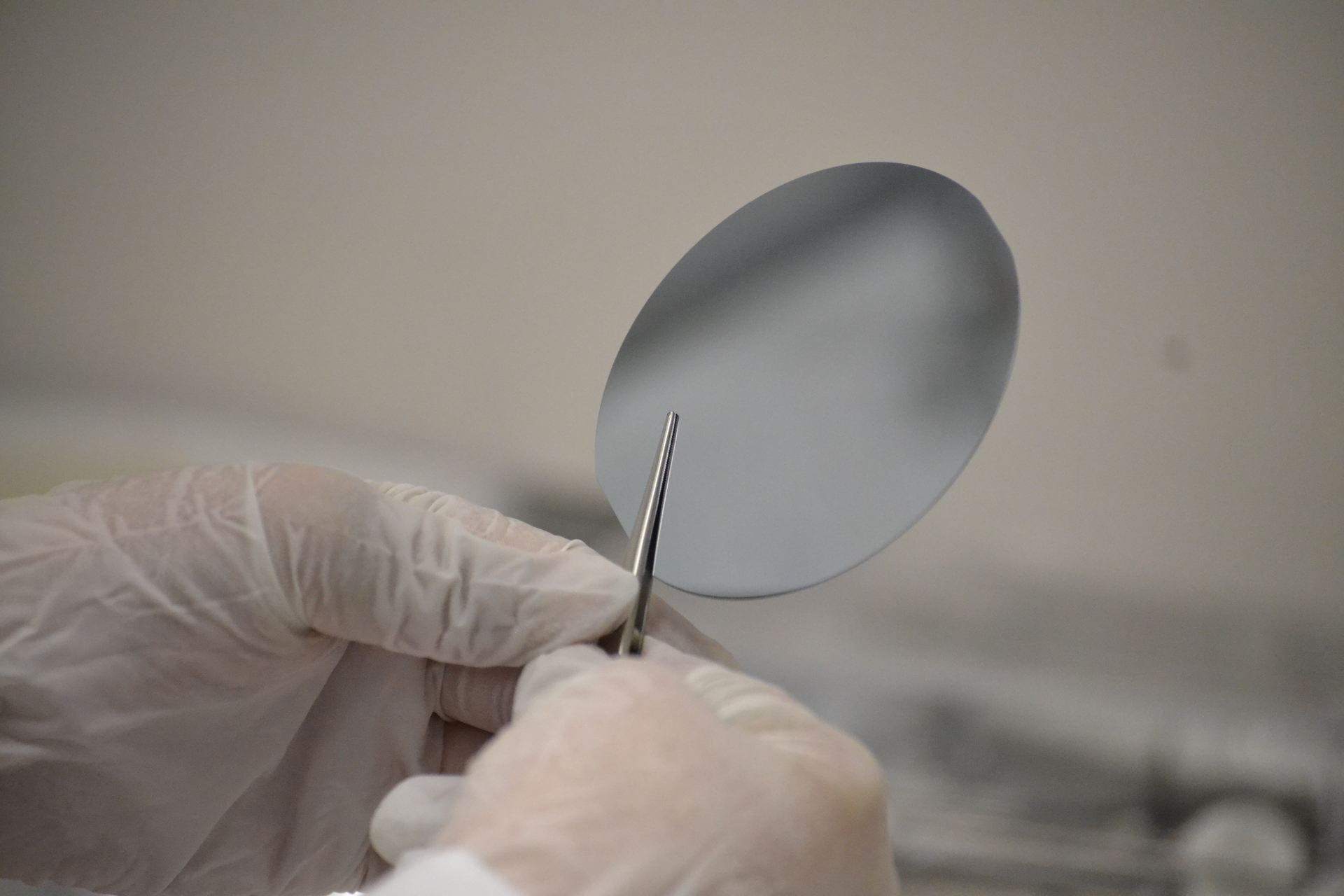
The University of Delaware (UD) Materials Growth Facility (MGF) offers III-V and topological insulator (TI) growth of epitaxial semiconductor films.
These growths are performed on a dual-chamber GENxplor molecular beam epitaxy (MBE) system. Our staff offers full-service material calibration and growth, as well as training to perform MBE deposition.
The MGF is integrated into the Delaware Institute for Materials Research (DIMR), providing seamless materials growth, materials characterization, electron microscopy, and nanofabrication capabilities.
Questions? Please review our procedures letter or contact us directly via the app or contact info at the bottom of the page.

Capabilities and Services
Standard Calibrations
The following calibrations are standard. Time and materials spent performing these calibrations are covered by the facility. Calibrations outside these standards may warrant consideration as a collaborator, or eventual inclusion as a standard calibration in the future.
- III-V MBE
GaAs growth rate, AlAs growth rate, InAs growth rate - GaSb growth rate, AlSb growth rate
- InGaAs lattice-matching (to InP)
- InGaAs growth-rate calibration
- InAlAs lattice-matching (to InP)
- InAlAs growth-rate calibration
- Silicon, Beryllium doping calibrations in GaAs (generally, convertible to other materials)
- Tellurium doping calibrations in GaSb
TI MBE
- Bi2Se3 growth rate
- Bi2Te3 growth rate
- In2Se3 growth rate
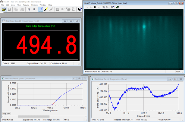
Growth Monitoring
Both MBE chambers have RHEED systems. The III-V MBE also has optical pyrometry and kSA BandiT band-edge black-body emission and thermometry for a wide range of growth temperatures.
Nanofabrication, Characterization, and Microscopy
The UD Nanofabrication Facility (UDNF) enables researchers from academia, industry and government to create devices smaller than a human hair, supporting scientific advances in fields ranging from medical diagnostics to environmental sensing to solar energy harvesting.
The UD Advanced Materials Characterization Lab provides opportunities for researchers with in the UD community as well as other Educational Institute and Industry. Equipment list includes: X-ray diffraction, thermal analysis, porosity & particle size, vibration, and mass spectrometry.
The W. M. Keck Center for Advanced Microscopy and Microanalysis (Keck CAMM) houses two 200 kV field emission transmission electron microscopes, two scanning electron microscopes (with FIB-SEM dual beam capability), and two scanning probe microscopes.